Going to a new home

In my last, brief post, how time flies.., I mentioned that plans were afoot to move my creaky, old, website to WordPress. Well it has finally happened. This blog has been copied to http://ianstedman.co.uk/blog-stuff/.

I’ll shortly delete the rest of this blog so I only have the information in onw place and will post new content there soon.

How time flies

My previous post on here was November 2018, yikes! I had not forgotten about this blog, just did not have a great deal to write. This blog will soon be moving to a new home, I’m planning to migrate my website to WordPress and will move the content from this blog to the new website.

I currently use the creaky, unsupported, Netobjects Fusion 2015 for creating http://www.ianstedman.co.uk, this was fine when I started the website back in 2002 but in 2021, it is slow and clunky and the pages don’t work too well on mobile browsers. I like the simplicity of WordPress so I will migrate soon.

What else have I done?

I discovered the joys of 3D printing, I bought my first printer, a Creality Ender 3 in December 2019 and have made good use of it. One worn nozzle, new extruder and a new set of bearings are testament to this. I have started to design a few gadgets myself, I use Fusion 360 for the 3D CAD as it just works for me. I’m not a great fan of the new Autodesk licensing but I’ll take advantage of the free Fusion 360 tool while I can.

I have started migrating away from Autodesk Eagle CAD for PCB/schematic design, I finally used KiCAD for a design, my open source RC sound effects design is now on Github, https://github.com/istedman/RC_Sounds. Take a look at my other designs on Github.

Outside of electronics/engineering I’m a keen amateur photographer. I’m a member of a local club in the south-east London area and regularly take part in competitions. I have even won a prize or two. My preferred camera is an Olympus OMD-E-M10 Mark II and my backup day to day camera is a Huawei P30 Pro. Mentioning that I use a mobile phone upsets some photographers but the latest ones take some damn good photos.

The next update will most likely be once I’ve merged this blog and my legacy website, so stay tuned.

It has been a while….

I have not forgotten about this blog, have been a bit busy with some other projects, a few details of which I’ll share.

I don’t do a lot of project development during the summer months, heck we had a decent summer in the UK this year, as I like to get out and about. I race radio control cars and boats, which is great fun. This has also given me some project ideas. I have a tripped out Tamiya Lunchbox monster truck, with up-rated motor, suspension and lights, the next step is an engine sound effects unit. I have a crude Arduino based system with a Class D amplifier that changes pitch depending on throttle. It kind of works but the sample size is limited and difficult to change, it uses Wav2c for the sample. I plan to change the design to use PCM audio files which can be handled by an Arduino. Work will continue over the winter. Not every project approach was right nor does it work first time. It was educational though.

I like my projects to use minimal components in a project, the simplicity and getting everything I can out of a Micro like the Atmega 328. It also makes it cheaper.

The other RC design, currently in the concept stage is a R/C assistant tool. The idea was borne earlier this year when I took my boat to the lake in Herne Bay, and when I got it out, nothing worked! I was 70 miles from home with limited diagnostic tools, all I had was a multimeter, not much use for a dead boat once I had verified power was present and correct. What I needed was something that could detect the presence, or lack of, the pulse width modulated signals between the modules. As well as detecting the presence of the signals, it also needs to create test signals to allow swapping in of known good sources. A microcontroller can easily do this. I would also want it to measure battery voltages to allow testing of 1-4 cell LiPo batteries. Such a device should help with most track side/pond side issues and hopefully allow for more successful days out.

The problem with my boat was due to the transmitter failing. The electrics went into Fail-safe mode. A cheap replacement radio system fixed the issue but I could not diagnose the fault until I got home.

If anyone reading this is also in to R/C and would be interested or has some suggestions, please contact me.

I originally started this blog to discuss projects in development for the Amiga retro computer, this still goes on but at a slower pace. I still manufacture the adaptors for power supplies and floppy drives for the Amiga and Atari computers and will continue for a while yet. Brexit and the poor UK exchange rates have pushed up my manufacturing costs by 25% over the last year, so I have had to increase my prices by 20%. I try to keep the costs down to be competitive but when you are only making small batches it can be difficult to get the costs low enough. I don’t make much from this endeavour, any profits are reinvested in developing new designs and financing the next production run. I do it as a service to the retro computer fraternity.

There are other ideas being progressed, the less is more approach will continue so as to avoid disappointment.

I have been asked numerous questions about the GBS8200/8220/HD9800 converter boards. I try to keep the comments moderated and I thank those who have answered some of the queries on this blog. Have you seen the great work on gbs-control project?
I have been asked about designing an improved GBS-8200 board based on the Tvia 5725. It’s a good chip, not necessarily programmed correctly, evident in the issues with motion in video games. Personally I would not use this for a video converter card of my own. These video chips are very complex. The last group of devices I used professionally took around 500 hours to develop and test a product for. You can probably see my reluctance to entertain the idea of a video converter card.

The problem with video devices, be they decoders (that convert analogue or digital video to a pixel stream) or encoders (that convert the pixel stream back to either analogue waveform or packet based/low voltage digital signal) is that the datasheets and manuals already assume you know how they work. Motion estimation, de-interlacing, chroma edge enhancement, 3D comb filters, PLL programming/coast time all have a major impact on the end video image. I should write some more on this in another post, when I get the time. Sometimes you need to play with these settings, but use the right source material to fully test them.

The TVIA5725 outputs analogue VGA by default, this was fine  back in 2011 but for 2018 and beyond, any solution needs to have an HDMI output. You can convert VGA to DVI/HDMI with another adaptor but it’s much neater to do it in one or two chips and avoid extra cables.

I will try and post a bit more often, stay tuned folks.

Too many spinning plates

Sorry I have neglected this blog for over a year. I’ve come to realise I have too many ideas on the go at once, which whilst great for variety, does not allow much progression. I took a long hard look at what I was doing and I have suspended all work on project Hermes (CD32 expansion) indefinitely. It was not due to technical issues, it was due to support. The original intent of the project was to produce 100 assembled and tested PCBs and then via a third party, sell them, I had a tacit agreement on this. The realisation, in part driven by bad experience in the day job, was that a more complicated design than a ‘simple’ ATX or floppy adaptor, would take a significant amount of my time to support. Currently I spend 8-10 hours a month dealing with enquiries, order packing and support requests for the products I currently sell. Allowing for a design that is more 4-5x more complex with more variables, I can easily see that the support time will increase considerably, easily to 10x the current level. When (not if) it gets to that level of effort, it becomes more of a chore than a fun hobby. This is the time to stop.

I will continue to support the products I currently sell. There are two small, Amiga related, projects, in the final stages of development. Will release details when they are ready. Once released and manufactured, they will be the last Amiga specific projects I work on.

The other projects I work on are increasingly micro-controller based and two of them use CPLDs for video and logic functions. These projects are more generic retro projects. I also develop designs for Radio Control systems, more on this when I finish them. Like most of my current projects, all the design data will be publicly available.

I realise this announcement will disappoint some people. Over the past 10 years, I have, on average, finished 7 projects a year. The past year, I’ve done 2. I’m older now and life has other distractions so I’ve decided to do what is best for me and to actually achieve success on smaller, more manageable projects rather than failure on one large project.

Thank you,

Ian

Synchronise your video engines

The importance of applying the correct video sync signal to your TV, monitor, scan converter, HDMI adaptor or projector.
This post tries to answer some of the many questions I get relating to the GBS-8200 and non-standard video types. I will
provide information on how to help identify the correct synchronisation or sync signal for shortness, for common applications
and describe some of the effects you may see when you get it wrong. I do not have a guaranteed fix for any problem, this is more
a how to guide to help you fix any issues you may encounter.

Topics covered in this post

What are synchronisation(sync) signal(s)?
Understanding your composite from your H/V and Sync On green type?
Basic information on video sync timings, PAL, NTSC, CGA, EGA, VGA.
Converting video sync amplitude
Sync strippers/cleaners/separators
Best options for the GBS-8200

What are synchronisation(sync) signal(s)?

Let’s start with a basic description of a sync signal. I took the following from the Tektronix Video Measurements glossary:

Sync – a) Abbreviation for synchronization. Usually refers to the synchro-
nization pulses necessary to coordinate the operation of several intercon-
nected video components. When the components are properly synchro-
nized, they are said to be “in sync”. b) Signals which control the sweep of
the electron beam across the face of the display. The horizontal sync, or
HSYNC for short, tells the display where to put the picture in the left-to-
right dimension, while the vertical sync (VSYNC) tells the display where
to put the picture from top-to-bottom. c) The portion of an encoded video
signal which occurs during blanking and is used to synchronize the opera-
tion of cameras, monitors, and other equipment. Horizontal sync occurs
within the blanking period in each horizontal scanning line, and vertical
sync occurs within the vertical blanking period.

With the move to LCD displays we are not concerned with movement of an electron beam but it is useful to understand how
the horizontal and vertical sync signals play their part in creating the display you see.

Basic information on video sync timings, PAL, NTSC, CGA, EGA, VGA.


Video type Horizontal
frequency
Vertical
frequency
Interlaced? Number
of lines
Notes
 PAL  50 Hz  15.625 KHz  Yes  576 active  (1)
 NTSC  59.94 Hz  15.750 KHz  Yes  480 active  (1)
 CGA  60 Hz  15.750 KHz  Yes  200  TTL signals. (2)
 EGA  60 Hz  15.750 KHz/21.80 KHz  No  350?  Vertical frequency changes depending on the mode,
200 line display is 15.750KHz, 350 line display is 21.80 KHz. TTL signals
 VGA  60 Hz  31.469 KHz  No  480+  Lowest resolution shown, extends up to 2014×1536

(1) Quite often when a system states PAL or NTSC output, e.g. a camera, the signal is a composite video signal. For higher quality
conversions, either a Y/C(S-video) or an RGB output is preferred. The sync is embedded with the video.
(2) CGA is unique in that it uses TTL digital signals, with an intensity pin to get 16 colours. If you don’t have an adaptor board to convert
the RGB+intensity to analogue, most converters will struggle. Has separate H/V syncs

You will note that I state that NTSC has a vertical frequency of 59.94 Hz, where as most of the other standards are 60Hz, indeed some
literature states 60 Hz for NTSC. In practice, most of the time this 0.06Hz deviation makes no difference.

Understanding your composite from your H/V and Sync On green type?

So you have a retro game console or computer and you want to connect it to a modern LCD  display or a projector, should be straightforward right?

Depending on the equipment you may have a single signal or multiple types. The table below details the main types:

Sync type Voltage Description
Composite video 1V Normally a yellow plug, contains video and a combined sync. Used by SCART inputs.
CSYNC TTL (2-5V signal) Output by some graphics cards or a TTL signal from retro equipment. It only contains timing information, no video.
HSYNC TTL (2-5V) signal Provides the horizontal video timing, which details the start and end of a line.
VSYNC TTL (2-5V) signal Provides the vertical sync timing, which describes the frame rate.
Sync-on-green 1V A -0.3V sync signal attached to a 0.7V peak green video signal.

An important point is that you need to know what signal amplitude is expected by your TV/monitor/scaler/converter. A common mistake, is to connect
a CSYNC signal, either from a retro device or a computer, to a SCART socket. The SCART standard expects composite video on pin 20, if you feed in a
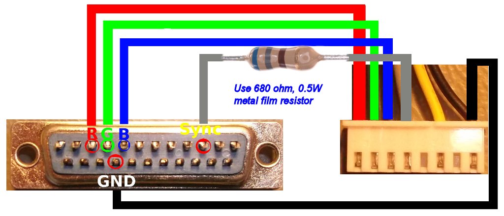
TTL CSYNC signal, you could be supplying a signal upto 5x higher than expected. My Amiga SCART  and Atari SCART cables fixed multiple video issues,
with a simple fix to the sync amplitude, by adding a series resistor on the sync signal.

I show a TTL signal as a 2-5V signal, for good reason. A retro computer or video system will have 5V logic, a logic 1 output can be from 2.4V (min) to 5.5V(max).
When you connect one of these signals to a 3.3V video chip, like that on the GBS-8200, you are damaging the device as the input signal exceeds the supply voltage.
The ESD protection diodes conduct and soft of allow the system to work, but they are not meant to be used continuously and will fail, at the same time as your board.
The next section details various methods of converting sync signals.

Converting video sync amplitude

So how do you convert a composite video to separate h/v sync or reduce a 5V TTL signal to 3.3V LVTTL or any or a number of options?

Some conversions are simple and can use readily available modules, others need a little circuit board. The table below will help:

From To Solution
Composite  CSYNC (3.3V or 5V)  Sync stripper
 Composite  H & V Sync (3.3V or 5V)  Sync stripper2
 CSYNC  Composite (1V) level  Resistor circuit
 H & V Sync  CSYNC (3.3V or 5V)  OR/XOR gate
 Sync on green  CSYNC (3.3V or 5V)  Sync stripper2
 Sync on green  H & V Sync ((3.3V or 5V)  Sync stripper2
 5V TTL  3.3V TTL  Level converter

Examples of each circuit element are shown in the sections below. What is not shown are power supplies and connectors. This is left to the developer,
though for all circuits shown, a simple linear regulator would suffice.

Sync strippers/cleaners/separators

When I first started researching video adaptors and converters I came across ‘sync strippers’ and wondered what they were. They are relatively simple
circuits, based around commonly available  sync separators, the most widely used being the National Semiconductor (now Texas Instruments) LM1881.
They accept a composite video signal and strip the colour burst off the signal and in the case of the LM1881, output a 5V TTL CSYNC signal.

Syncstripper circuit

LM1881-circuit

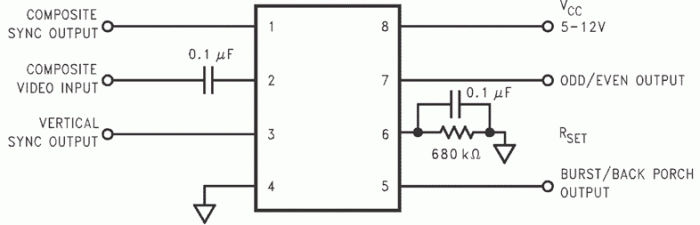
Taken from the LM1881 datasheet. Widely used as it’s a readily available part in a DIP package.
There are two limitations of this part:
1) The 5V TTL output is not compatible with modern TVs/HDMI adapters/projectors. It needs a level translator.
2) It does not provide a separate horizontal sync output. If your adaptor only needs CSYNC, great, otherwise try the Syncstripper2 circuit below.
You may get away with using CSYNC for HSYNC but it is by no means guaranteed.

Syncstripper2 circuit

LMH1980-circuit

Again taken from the datasheet. Being a surface mount device will put some people off, the VSSOP-10 package is a bit small but you can
easily buy a SSOP to DIP adaptor off ebay. If you power it from a 3.3V supply, the logic level outputs will be compatible with modern
display devices, no external converter needed. It provides true H/V and C sync outputs and works with a wider range of video types and frequencies.

Would an adaptor board with this circuit, video amplifier and maybe a scanline generator be of interest?

Potential divider and logic level converters

Resistive potential divider circuits
The first circuit converts 5V TTL signals to 1V CSYNC for SCART

5VTTL-SCART

This is a simple potential divider circuit. The output voltage is 75/(75+330) x Vin which gives an output voltage that is ~18% of the
input or around 0.92V.

The second variant is for the GBS-8200 or a modern monitor that is not 5V tolerant.

5VTTL-LVTTL_resistors

With a VESA VGA video monitor or equivalent, the input impedance of the display is much higher, in this instance, 2K. As the aim is to
reduce the signal to be approximately 3.3V, we reduce the amplitude by 27-30%.

One disadvantage of this circuit is that the RC time delay does affect the rising/falling edge of the sync pulse slightly. In most circumstances,
this will not matter but some systems may have issues if the time delay extends past a 100ns rise/fall time. For a cleaner, faster signal, use
logic devices.

Transistor logic level convertor

An improvement is to use a transistor circuit.
FET_level_Translator

This circuit is simple to implement and provides faster edges than resistor networks. You will also find this on ebay as a
level translator for the Arduino, it is acceptable to use it for video.
LevelConverter-L


OR/XOR sync combiner circuit
HV_Sync_Csync

The circuit shown above has the option to use either an OR gate or an XOR gate to combine separate HSYNC and VSYNC into a CSYNC signal.
Most of the time, the OR gate will suffice. Depending on the display you interface, you may need to invert the vertical syn portion,
hence the option to use an XOR gate. The 33R resistors were added to damp any ringing when driving long cables. With careful selection of the logic
family, you can use a 5V tolerant part, operating from a 3.3V supply.

Effect of supplying a 5V signal to a 3.3V device

This could be very detailed and lengthy discussion detail the effects of electromigration and it’s detrimental impact on device reliability. I’ll summarise,
DON’T CONNECT 5V LOGIC TO MODERN MONITORS OR ADAPTORS!
Whilst it will appear to work, you may see odd effects, occasional display artefacts or issues displaying a stable image occasionally. If a device is powered
from 3.3V and you feed in 5V, you are exceeding the power supply by upto 1.7V, not a good start. The internal ESD protection diodes, will clamp the signal
to around 3.9/4.0V, which you might think is OK. The clamping action distorts the signal and can cause the video display/adaptor to incorrectly sample the sync signal.
The ESD diodes are only meant to  have short term use to protect from static electricity, which is normally a short, sharp shock. If they are continuously used, they
will fail and when they do, the full 5V signal is fed into the IC. Depending on many factors, the distortion will get worse but one thing is 100% certain, the device will fail.

Best options for the GBS-8200

I would recommend as a minimum that any sync signals are scaled using at least a potential divider circuit or a transistor level shifter as they are readily
available, providing your source produces a C sync signal. If you need to to combine H and V Sync, use the logic circuit shown above.
If your system provides a composite video signal, use one of the sync strippers but ensure you condition the output to be 3.3V LVTTL compatible.

Summary

I hope this guide has been useful and informative. It is only meant to provide guidance on common issue I have encountered when inter-connecting various video
systems it is not a definitive guide of what you must do. Sometimes you need to experiment, if you have an oscilloscope, make some measurements.

I’ll be taking a break for a bit whilst I get busy with the CAD tools but I will read and respond to your comments.

May the 4th be with you

Forgive me it has been six months since my last posting, I have been a little busy.

Project Hermes is still in development but has progressed nicely. I started my review work on the design back in March 2016 and made a few tweaks to the design. The review schematics are  here: Hermes_development. One of the principal design requirements was to make it work within the CD32 power/space/performance envelope. One are the design was struggling with a little was power. Most of the anticipated power consumption was in the 5V to 3.3V converters for all the new logic and 2xCPLDs. One evening, with some help from Ti’s WEBBENCH(R), I had a solution that nearly halved the power consumption of the card. The BOM and schematics were updated accordingly.

When you look at the circuit on page 3 (which is not sexy), you may wonder why that was a few hours work. Component selection, simulations, schematic and BOM updates take time but the task is now done. This is one of many little tasks to complete.

The biggest challenge has and still is the programmable logic. I have a preliminary design which needs a test bench to prove it. I have ‘re-used’ some concepts from other projects but very little code. A few designs I looked at for the 6800/68020 processor bus used asynchronous logic. Whilst this will work, it does have the potential to cause a metastability problem. As someone who works with high integrity hardware, the design needed to be changed to a synchronous system. To speed up the logic decode, a 28 MHz clock is generated from the 14 MHz clock provided by the CD32. This ensures I have a higher speed, time aligned, clock for the logic decode and to help reduce the need for wait states. It does not convert the design into an accelerator!

It was whilst developing the programmable logic that a clash of projects occurred, something which took time to effectively resolve.

One of the features added by the MIA CPLD was the floppy disc interface. The core design was based on the CD32 floppy design on Aminet. One of my other projects was a prototype floppy interface in VHDL for the classic Amiga. It made sense to finalise that design before incorporating that design into Hermes. The basic double density only design has been incorporated after the final compliance testing was integrated with my A1200. In the near future I plan to release the V3 floppy interface, with the highly experimental, HD support. If I can get the HD support working reliably, it can be incorporated into Hermes.

The second conflict was from my Retro Video Adaptor, another project, which looking at that page, has gone nowhere since 2013. It’s not the whole truth it stalled for good reason, it would not work reliably with 240p/288p video. The basic concept was fatally flawed. It was inspired great success achieved using these video decoder parts with non-standard video but the tricks I learnt did not work with the Amiga! Without using timebase correction on the video output, I could not get YPbPr or HDMI outputs to work reliably. It was from this issue that I initially started playing with the GBS-8200 as this has a timebase correction feature. The critical feature of the GBS-8200 is that it has a framebuffer memory to convert the 240p(NTSC) and 288p(PAL) video to a higher resolution and provide a 60Hz output at a standard resolution. Without a stable output conversion, the downstream video output can not be converted to YPbPr or HDMI. It is this issue with 240p/288p video that causes many SCART to HDMI adaptors to fail as they do not know how to handle this video system. Some will interpret 240p as 480i (NTSC) and de-interlace, thus causing fuzziness. The same goes for 288p being interpreted as PAL video. Switching off the de-interlacer greatly improves the GBS-8200 video output with 240p/288p.

Tecnobabble out of the way, how is this relevant to the long delays on Hermes?
I have been looking into incorporating an HDMI output into the design. Handling the audio is easy, I have a stereo audio ADC for that that outputs the correct transport stream, it’s just the Amiga video I need to solve. Some experiments with a small FPGA to ‘adjust’ the timing were trialled with no success. Experimenting with the GBS-8200, I have seen what a system that can re-time and re-scale the video can achieve, whilst being fully aware of the issues of motion compensation and blurring among other artefacts. It was with regret that the implementation of an HDMI interface will not be part of the Hermes design. This decision was made due to the amount of time required to implement a reliable interface. It will be better to run the two projects in parallel and maybe add this in at a later date if a solution becomes viable. I have a candidate solution which is undergoing technical evaluation.

Someone will ask why don’t I use the Vampire FPGA accelerator and HDMI core?
The HDMI output is incorporated into the CPU core design and associated FPGA. The Vampire design is a very clever implementation but currently only supports 68000 instructions, the CD32 has a 68EC020 which supports a slightly different instruction set. The other reason is that at my current development rate, adding a new FPGA accelerator the design would never be finished!!! :p

The third and final conflict was finishing the updated Amiga/Atari floppy adaptor. I’ve just sent out the purchase order for a production run of 75 units. Yes you did read that correctly, the new design has been updated to work with the Atari ST/TT/Falcon in double density mode. This was a late design addition that delayed production by 2 months whilst a new prototype was successfully built and tested.

What’s next?

I still have a few changes from my design review to incorporate, mainly to improve testability and reduce emissions. Once complete, I’ll finish tracking the PCB. The prototype PCB will be a six layer PCB, this will make it easier to track and to provide some controlled impedance signals. Experience gained from getting the existing adaptor PCBs has helped me find lower cost quality PCB suppliers and assemblers.

I’ll answer another question, why have I not just made a prototype of the design I had 6-9 months ago?

Cost. A batch of 3 assembled prototype PCBs would cost >£500. It would be a bit cheaper if I assemble the prototypes myself. I’d rather spend a bit longer doing my innate design checks/double checks before committing to a prototype.

I will try and update this blog more often. There’ll be another post shortly related to the GBS-8200 experiments.

May the force be with you!

Being creative on cyber monday

It has been some time since my last post, I meant to post earlier but got a bit distracted reviewing and deleting 24 emails and text messages I had regarding Black Friday! Cyber Monday added another 16 emails. Decided to be creative and write another blog post instead.

First of all, after a few unforeseen delays, the ATX power adaptors will be available soon. My expected delivery date from the manufacturer is 25/12/2015, a nice early christmas present! It will take a few days to get the boards programmed and tested once complete I will list the adaptors for sale on my website. Realistically, it will be January 2016.
The CDTV ATX adaptors are in stock, as are the audio mixer PCBs.
The smaller floppy adaptors (for double density Amiga use) will follow in approximately 2 weeks, so middle of January. A late change for further use, has delayed sending this order out to manufacture.
Pricing is largely unchanged:
CDTV power adaptor £9
picoPSU adaptor £10
Mega adaptor (replaces original and big box) £11
Audio mixer PCB £4
Postage and packaging to be added to all orders.

Getting PCBs fabricated is easy, I have used multiple vendors with comparative ease. Getting PCBs fabricated and assembled, for a reasonable price is another story. I contacted 7 companies for quotes and only got responses from 2 of them. I guess small quantities (75 of each PCB) was too low for some of them. The company I chose to manufacture and assemble the PCBs has been good, so far. With a few minor changes and advice from them I managed to remove one of the higher costs from the Mega adaptor PCB by removing the need for 2Oz copper to take the power, this halved the PCB costs. Hopefully I will not be disappointed with the assembled units when they arrive at Christmas.

I do try and respond to comments on the blog as soon as possible. I added the information regarding my upcoming projects to try and reduce the number of ‘is it done yet’ emails I’m getting. This blog and my development projects are a hobby activity, I have a full time job working in the electronics industry, so sometimes it is necessary to take a break from electronics! Sometimes work is not fun but at least I get paid to do it, if the ‘hobby’ ceases to be fun, it’s time to stop and do something else. I am committed to my current projects, just taking my time to get them right 😉

Project Hermes is one of my more popular projects, the current quick status is this:
Schematics complete and in internal review.
Changes made to fix potential EMC and signal integrity issues.
First draft PCB layout in progress.
Feeding in some lessons learned to reduce the PCB costs

ETA 2016. See my comments in the previous paragraphs.

The other project I have many comments about is regarding my experiments with the GBS82XX video cards and retro games hardware. I started developing an Arduino programme/sketch that reads the numerous status registers, decodes the input video type and then sets the correct output display. I had a bit of fun with 3.3V/5V I2C interfaces, fixed with a cheap level converter from Squirrel Labs. It needs a lot of work to finish the basic input testing and resolve a few bugs and is not currently in a format to release. I know what I need to do and roughly how to do it, but I can’t release anything yet as it will leave more questions than answers. This will be a nice project to experiment with over the Christmas break!

I’m not going to respond to any further questions of ‘can you make this work with system X’ or ‘why does this not work with my antique video system Y’. Sorry to be so blunt but I have other things to do. I am working on my retro video guide, which when finished (and published on my website), will help you to resolve the more common issues and hopefully give a better understanding of the vagaries of video.

That’s all for now, I plan another update by year end, hopefully with some pictures.

The benefits of prototyping, even the smallest of designs.


As the existing stock has being cleared, it needs to be replenished, progress has been made to do this. The Retro ATX adaptors (not Amiga specific now), have been prototyped and the first two prototypes assembled as shown here

New_ATX_2015-medium

On the left is the small form factor design, primarily aimed at the picoPSU ATX power supply. On the right is the multi-purpose ATX adaptor (formerly Big Box), aimed at higher power systems and those that require additional features, notably -5V supply, 50/60Hz mains tick and AC fail status.

Some of my regular customers will notice a move away from the Amiga specific titles. The reason is simple, these adaptors will work with multiple retro systems, a name change can help generate more sales and of course happy customers. This has in part been driven by feedback from customers, asking if these adaptors work with other systems, the answer is yes. If you have a vintage retro system, with a 1980’s power supply, you may be at higher risk of power supply failure due to aging effects due to heat and dried up electrolytic capacitors. Replacing your old power supply can provide some peace of mind.

I will provide details on wiring up these adaptors for various Retro systems, including the BBC Micro, Apple II and Sam Coupe among others on my website in due course. It is not viable for me to supply power adaptors for systems that require a 9V DC supply, like the Oric Atmos or Sinclair Spectrum, as you can easily purchase modern switchmode converters.

For low power systems, I recommend a genuine picoPSU adaptor, manufactured by Mini box. Unlike most high power ATX adaptors, these converters have no minimum load requirement and are silent. A typical 230W+ power supply will have a minimum load rating, to ensure the outputs are stable so to use a regular 230W+ power supply with a retro system, using 25W, you need load resistors, sometimes dissipating upto 25W of power!

The prototype PCBs were ordered from a local company, Ragworm, hence the orange silk screen. The build quality was very good and it took me just over an hour to assemble the boards. As the aim was to get these PCBs assembled by a contract manufacturer, the existing designs needed a few refinements. All components are now on one side of the PCB, this reduces the number of process to 2 (SMT load top side and hand solder) from 3 (+SMT bottom side). This saves on the recurring costs. The control electronics have been simplified, reducing the part count. All control is now via a Microchip PIC10F202 micro-controller in a tiny 6 pin SOT023 package (3mm x 3mm), programmed on card via an ICD 3 programmer. This allowed for easy configuration for momentary or latched power switches and improved de-bounce compared to the previous design. It also provides a 50/60Hz square wave output, useful for some Amiga models that require a mains ‘tick’ signal. Finally the design also switches on/off the supply.

On both boards, I have added extra, larger, pads for connecting your own power wiring in addition to a 2 pin header. On the multi-purpose adaptor, the number of +5V and 0V connections have increased from 2 to 4, making it easier to connect to a high power, 100W+, system (mainly Amiga 2000/3000/4000). Simple changes that were easy to implement.

What did I learn from these prototypes?

For the Multi-purpose adaptor, the text describing each power rail, by the screw terminals, should be rotated 180 degrees, making it easier to read when wiring up. The linear -5V regulator needs more copper area to act as a heatsink.

Order your programming cables long in advance! To program the PIC micro and save on recurring costs, I decided to use a Tag Connect, TC2030-MCP-NL programming cable, this only requires a tiny PCB land pattern on the PCB. It may not seem much, adding a 20p, 1.25mm connector to each PCB but on a batch of 200 PCBs, it certainly adds up. The annoying part is getting hold of the cables. I currently have a cable on back order from Farnell, expected delivery date is 10th August! Finding stock in the UK has been tricky.

The other prototype PCB has been the V2.5 Amiga floppy adaptor shown here:

New_Floppy_2015-medium

This board showed the benefits of prototyping. You may notice the orientation of the drive connector is odd?
I designed this board to have a reduced form-factor to easily fit behind the floppy drive, adjacent to the drive, this did not work. The problem was that some drives, like the Mitsumi drives in my collection, have the +5V power connector above the 34 way IDC connector. So with the PCB plugged in, you can not connect the power, oops.

This new PCB is 60x24mm, the previous (V2.1) PCB was 53x40mm. The ideas was to make it smaller to fit more easily inside the Amiga and to allow easy assembly into a case to act as an external DF1 floppy drive, either with a real floppy drive or with a HxC or USB (Gotek) virtual drive. Moving the design to Little Logic and 0603 surface mount components allowed me to make the PCB much smaller.

As well as the mechanical error with the power connector, it also highlighted a limitation of the Design Rule Checks (DRC) that I run on the PCB data. One of the floppy drive connectors (the white one in the photo) is too close to a couple of resistors, this could easily be damaged in assembly and would limit inspection and rework.

The production PCB will be 5-7mm longer and the same width as the IDC box header, the two jumpers, one on either side will move into the extra space.

I am learning how to use mechanical 3D design tools (Sketchup and 123D), as an electronic engineer, they have taken some learning. I do want to master one or both tools as a 3D printer is on my wishlist. Sometimes you can’t beat a real prototype though.

The PCBs shown above need further testing before I release them for manufacture in batches of 100 of each design. The lessons learnt, minor in some cases, from these prototypes has been invaluable. Once the design release is complete I can get back to my other projects in earnest. Until the next post.

Ian

So what’s taking so long?

I’m sure the followers of this blog have been asking the same question.

Due to other pressures/commitments I stopped all development work for the first 5 months of 2015 and have recently resumed. There is a backlog of work and projects to finish, which is progressing.

The existing Amiga adaptors I sold have been updated, new, simpler,  ATX power adaptors are in prototype PCBs, once testing is complete, a production order will be placed. Likewise the floppy drive adaptor has been updated, the new PCB is much smaller and easy to manufacture. Have also updated the un-released V3 design to support USB/SD card floppy adaptors internally/externally and experimental HD support.

Previously the Amiga adaptors were hand made by myself. This was getting time consuming as the volume of orders was increasing, great for business but I was struggling to make enough in batches to deliver. To alleviate this, all new designs will be outsourced to UK based contract manufacturers. This leaves me more time to design and test products.

Project Hermes is progressing, I have the core of the MIA CPLD coded but not tested. The schematic took longer, due to my decision to use Designspark, which was a big mistake. After getting rather frustrated with the tool, I ditched it and went back to the familiar Eagle CAD software, which I can use. I’ve been using Mentor Graphics tools for 19 years, Eagle for 12 years and used OrCAD for a bit, Designspark was the worst I’ve used!

I’ve written the Arduino code for the GBS-8200 board to detect the incoming video and scale/de-interlace accordingly but have not tested it yet. It’s a lower priority project at the moment but one I want to return to in the future.

In my next update, I’ll show the assembled prototype PCBs of the Amiga adaptors and the complete schematics for project Hermes. Hopefully June/July time.

Regards,

Ian

GBS-82XX experiments part 2

GBS-8200 and GBS-8220 experiments part 2

Work has continued, experimenting with these low cost but potentially highly capable video adaptor boards.

Fixing the random speckles on the display

I believe I have found the cause of the occasional white speckles seen on the display. The default setting for the GBS-82XX board is to clock the 166 MHZ speed grade SDRAM at 162 MHz. It appears to be worse if the Hynix HY57V643220DT-6 is fitted compared to the EtronTech EM638325TS-6G device, which appears to be fine.

I measured the SDRAM clock at 162 MHz and recorded this:

gbs-clock-small

Whilst the signal is a bit noisy, it does not violate the +/-2V overshoot/undershoot limits of the SDRAM devices used.

The simplest fix was to reduce the SDRAM clock speed to 129.6 MHz, with a single I2C write. This has fixed the issue. Halving the SDRAM speed to 81 MHz caused distortion on the video, the next speed increment of 108 MHz was sufficient for 1360×768 pixel output. A proper fix would be to adjust the timing of the DQM strobes with regard to the data bus as on SDRAM the DQM strobes clock the data out of the SDRAM. If this is adjusted, you also need to consider the timing of the SDRAM clock to the control bus (RAS, CAS, CKE, CS, BS0/1 and WE) and the Data bus. This is not too difficult if you have the PCB artworks as you can measure the PCB track lengths and adjust the timing by 7ps/mm. With the GBS-82XX board, it would be tricky and fraught with false starts. We could of course measure it and adjust accordingly, or reduce the clock speed by 20% and have more timing margin (an extra nanosecond) on the clock.

Now that the speckling problem appears to be fixed, I am looking at some general video quality issues. When using a 50 Hz PAL screen-mode, scan-converted to 60 Hz, there are some noise bands, particularly noticeable on a grey Workbench background. It is hoped that some digital filtering/sampling will help alleviate this.

Synchronising the GBS-82XX

I have experimented with different ways to synchronise the GBS-82XX device. As those of you that have experimented with the board now, sometimes it can be a bit ‘hit and miss’ with the video source (games console or computer).

When using the GBS-82XX with the Amiga, this is the cable I use:
GBS-82XX-cable

The 680 ohm resistor is essential. It reduces the CMOS Composite sync signal from the Amiga to < 3.6V. The TVIA-5725, the device under the big heatsink, accepts a maximum voltage of +3.6V and a minimum voltage of -0.3V. The Amiga’s video sync, measured on the A1200, looks like this:Amiga_CSYNC_680R_GBS8220
The TVIA-5725 accepts a 3.3V TTL signal, via a Schmitt input, this changes logic levels slightly so a logic 1 is 2.4V to 3.3V,  and a logic 0 is 0 to 1.0V. The 680 Ohm resistor works as the GBS-82XX follows the Vesa VSIS specification, which requires synchronisation inputs to have a 2K impedance to ground. My 680 ohm resistor (+47 ohms in the Amiga), creates a potential divider, reducing the signal level to a safer level. This is cheap and easy to implement and does not degrade the video sync significantly.

A number of people use the venerable LM1881 video sync separator, any device or circuit that uses this, should have the 680 ohm resistor added as shown above. The LM1881 outputs 4-5V sync levels that are not compatible with the GBS-82XX/TVIA-5725. Alternative devices are the EL1883 or the LMH1980 but they are not available in hobbyist friendly DIP packaging.

I have tested the LMH1980 with the Amiga, I used the composite video output of the A1200 to create LVTTL (3.3V) HSYNC, VSYNC and CSYNC. The GBS-8200 I have synchronised with the CSYNC perfectly, the same as using a resistor. It did not work reliably when I supplied separate HSYNC and VSYNC, I had a very wavy display.

A final note, the GBS-8200 did synchronise to the Composite video output of the A1200 but it is not recommended. The 2V (approx) video contains colour information that is not filtered out and would in all eventualities, cause problems at a later date.

Cleaning up the power supplies

I have been reading numerous web-forums on GBS-8200/GBS-8220 problems to look for common trends and solutions. One topic that crops up a lot is related to the power supplies. I have already proven, in part one, that a 5V 2A supply is not required.

During my testing, I noticed an occasional, high frequency, burst of noise, on the +3.3V supply. I traced it back through the circuit to the power input. Changing the timebase of the oscilloscope, I spotted something important, it happened at 20ms/50Hz intervals. In the UK and Europe, the AC mains operates at 50Hz so when you see a 50Hz noise pulse, you know where it came from. Currently my GBS-8200 is powered from my bench power supply, built 20 years ago, with 3 linear regulators and still on the original electrolytic capacitors.

Also connected to the +5V output was my 5V to 3.3V TTL buffer board. Two of the eight inputs were in use, the other six were floating. I made a mistake here. You should never leave TTL inputs unconnected, they will pick up noise and oscillate, in this instance, they picked up 50Hz mains noise. Quickly dis-connecting the buffer board, removed the noise. The 3.3V (switchmode) and 1.8V (linear) regulator supplies now have about 20-30mV of noise, perfectly acceptable.

To ensure I do not have any further conducted noise issues I added a clip on ferrite bead:
GBS_with_ferrite

You can see the buffer board in the top right of the photo. Whilst this ferrite was a little large, it did cut the noise out. If you are using the DC power jack (the black plug) either pick a PSU that has a ferrite fitted or measure the cable diameter and purchase a clip-on ferrite from a local supplier or ebay. I spent two hours trying to work out where the noise was coming from, reading datasheets and measuring the board.

To date I have changed a single capacitor on the board. I briefly touched on this in my first post but after additional testing, I am happy to confirm it needs changing.
Here it is:
Capacitor_to_change-medium

The 1.8V regulator is used for the core supply of the TVIA-5725. with a ceramic capacitor, I was able to cause the power supply to glitch by switching my overhead inepection light on/off or my soldering iron transformer. Since changing it to a 16V, 22uF, tantalum bead capacitor, this has not happened. The original capacitor, shown under Kapton tape, had an ESR of 0.02 ohm, the recommended range for the LM1117 (similar to the AMS1117 used here) is 0.3 to 22 ohms! The part I fitted had an ESR of around 2 ohms.

The software settings solution?

Some people ask what the final software settings solution will be?

My preferred option is to use an Arduino Nano like this:

ArduinoNanoFront_3_lg

(Image from http://arduino.cc/en/Main/arduinoBoardNano)

This would be used to read and write the I2C commands to the TVIA-5725 device which provides the video scaling functions, among others. It is readily available and clones can be cheaply procured, finally it can be easily updated using the Arduino environment.

My aim is to make the design data readily available, for free. This will include the video settings. I’ve seen too many scammers on ebay selling ‘Amiga modified’ equipment for extortionate prices, I will not have this solution exploited.

Another option, still using the Arduino approach is a module that piggybacks on the 8051 microcontroller clone on the GBS board. This would allow access to the onboard switches and no wiring. The downside is it would be more expensive.

Until the final settings are known, the end solution is fluid.

Until the next update.